
Recently, there has been an increase in the usage of Integrated Circuit substrates by electronics engineers/designers. The main reasons are their mass production, lower costs, reliability, compact size, and effective electrical performance. Therefore, we will discuss their functions, manufacturing process, applications, substrate design technologies, etc., to learn more about IC substrates.
Table of Contents
- What is IC substrate?
- Functions and characteristics of IC substrates
- Classification of IC Substrates
- Features of an Integrated Circuit
- Application of IC substrate PCB
- How to manufacture IC substrate PCB?
- Technologies Involved in the Integrated Circuit Production Process
- Conclusion
What is IC substrate?
IC substrate is a baseboard type used to package bare integrated circuit chips. It connects circuit boards and chips while providing other functions, which we will discuss shortly.
Functions and characteristics of IC substrates
Function
Some of the critical functions of an IC substrate are;
- Providing heat dissipation channel, supporting, fixing, signal and power distribution, and protecting IC chips. They also act as intermediate PCBs and communication chips.
- Its internal circuit arrangement allows connection between the circuit board and the chip.
- Then, it carries semiconductor IC chips.
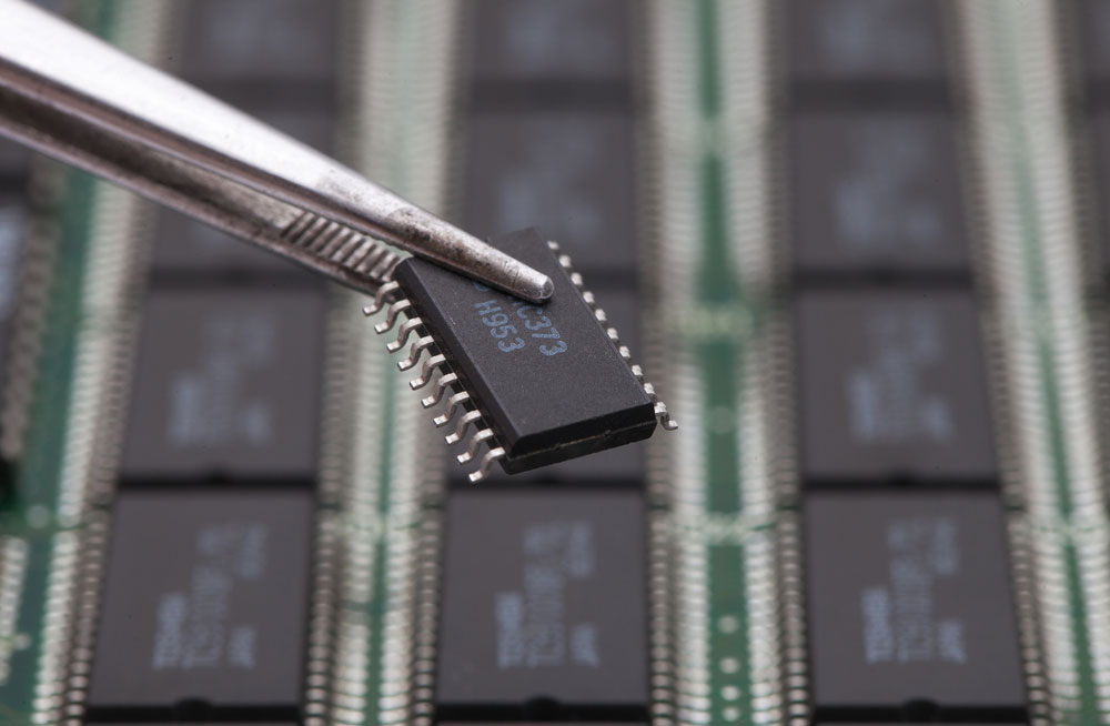
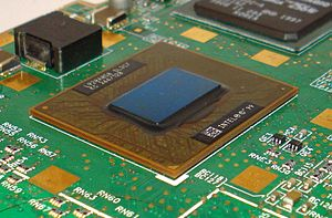
(IC chip)
Characteristics
- First, it is a single IC carrier with a board size of ≤150*50mm.
- Then, its surface coating comprises gold/palladium/nickel, hard gold, soft gold, Ni/Au, etc.
- Besides having a buried blind hole, impedance, and buried resistance capacity, it also has a contour tolerance ranging from 0-50microns.
- Its minimum ring width is 50microns, while its minimum pattern spacing/width is 10-80microns.
- Fifthly, its minimum aperture is 0.03mm in micro-hole, and 0.1mm in through-hole, whereas its minimum PCB thickness tolerance, is 0-micron.
- Finally, it has a board thickness of 0.1-1.5mm and 2-10 layers.
Classification of IC Substrates
Many IC substrates are in the market, each falling under a specific classification due to factors like packaging type. Let’s look into them.
Classified by package types
- BGA IC Substrate: It is an advanced packaging that performs exceptionally in thermal dissipation and electrical applications. Additionally, it is ideal for IC packages with more than 300 pins because it can drastically increase the chip pins.
BGA IC substrate packaging
Source; Wikipedia
- CSP IC Substrate: Besides having a miniaturized scale, it’s a single chip package type that’s light and suitable for memory, electronic, and telecommunication products with few pins.
- Flip-Chip Integrated Circuit Substrate: The FC IC package type has features like well-performed/effective thermal dissipation, low signal interference, and low circuit loss.
- Multi-Chip Module IC Substrate: MCM substrate encompasses chips with different functions in one package, thus offering perfect solutions like shortness, miniaturization, lightness, and thinness. However, it isn’t ideal for good routing, signal interference, or thermal dissipation because of packaging multiple chips into one.
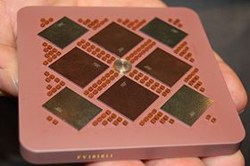
Ceramic multi-chip module
Source; Wikipedia
Classified by Material Attribute
- Rigid Integrated Circuit Substrate: Primarily, it contains epoxy resin, BT resin, and ABF resin. What’s more, its coefficient of thermal expansion (CTE) is about 13-17ppm/°C.
- Flex IC Substrate: It is a type of substrate with a CTE of approximately 13-27ppm/°C and primary constituents of PI and PE resin.
- Ceramic IC Substrate: Its ceramic substrate materials consist of silicon carbide, aluminum oxide, or aluminum nitride. Also, its relatively low CTE ranges from 6-to-8ppm/°C.
Classification by Bonding Technology
Includes;
- Tape Automated Bonding (TAB)
- FC Bonding
- Wire Bonding
Features of an Integrated Circuit
When aligning your IC with an IC substrate, there are particular features you need to have in an integrated circuit. The features of IC consist of;
- Miniaturized circuit; Often, the IC is small, meaning the debugging processes, installation, and design are usually non-sophisticated and uniform.
- Cost-effectiveness: Compared to other components, all ICs are relatively cheaper with higher performance.
- Reliability: ICs are highly reliable because they have reduced virtual welding and soldering joints. Consequently, their consistency and performance are commendable.
- Lower failure: You’re less likely to experience failure rates with ICs than with ordinary circuits.
- High efficiency and energy saving; Finally, integrated circuits consume less, making them energy efficient.
Application of IC substrate PCB
Integrated circuit substrate application is ideal for electronic products with advanced functions, thinness, and lightweight. Hence, they comprise;
- Networking applications in medical care, industrial control, aerospace, military, and telecommunications field,
- Electronic devices like laptops, smartphones, and tablet PCs,
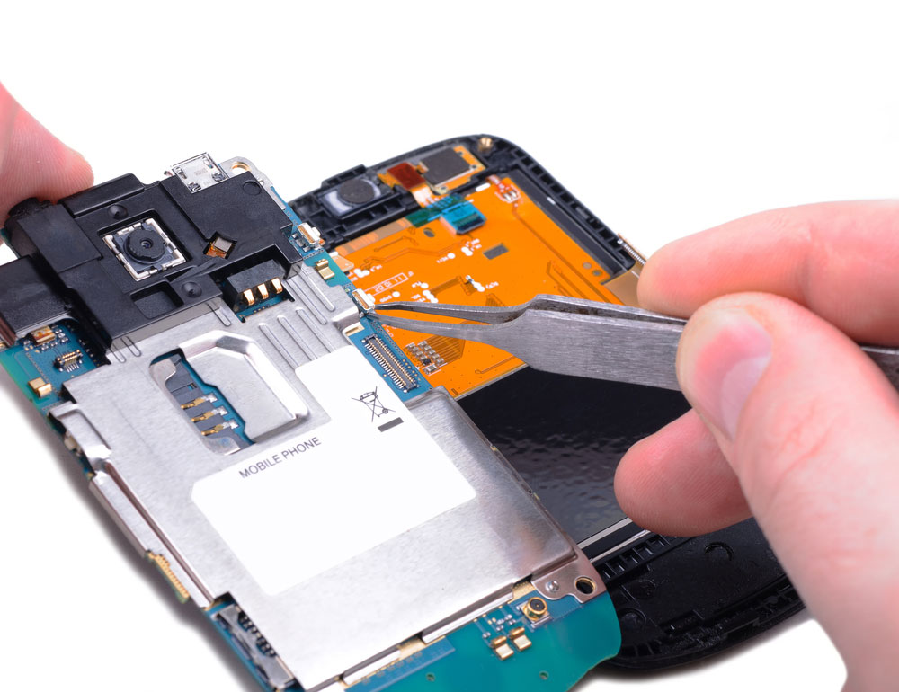
(Disassembled part of a smartphone showing the PCB)
- Automotive applications,
- Smart devices like smart wearables.
How to manufacture IC substrate PCB?
As we already know, an IC substrate primarily connects an IC chip and PCB using a network of holes and conductive traces. A snippet of the manufacturing steps is as follows;
- Copper plating and patterning: The first step involving copper patterning and platting technology correlates to other aspects of diverse technology. The tech includes fine-line fabrication, uniform copper plating thickness, and circuit and control compensation technologies.
- Solder mask: It’s the second process and comprises an IC substrate solder mask with solder mask printing and hole filling technologies. Remember, the substrate height difference between the pad and solder mask should be less than 15mm (ideal – 10mm and below).
- Surface finishing: It includes using ENIG and ENEPIG surface finishes (most common) to create a uniform thickness in the surface finish.
- Reliability and inspection test: Finally, design engineers test IC substrates for reliability and use dedicated modern equipment to inspect their quality. But the process differs from the ones used in standard PCBs.
Note; One technical difficulty you can encounter is a thin IC substrate that’s easily deformable. Fortunately, you can solve it by controlling the lamination thickness and substrate warpage through layer-positioning, lamination parameters, and board shrinking systems.
Technologies Involved in the Integrated Circuit Production Process
Some of the several advanced technologies in the IC production process include;
- Direct Imaging Systems
It handles challenging ball grid array/chip scale package (BGA/CSP), flip-chip chip-scale package (FCCSP), and flip-chip ball grid array (FCBGA) applications. Besides lowering the products’ total cost of ownership (TCO), the process helps manufacturers/fabricators gain higher yields.
Flip-chip BGA (FCBGA) chip
Source; Wikipedia
- Automated Optical Inspection Systems
Secondly, we have automated optical inspection systems that allow high-resolution, high throughput inspection in applications like IC substrates FCCSP and FCBGA. Further, it uses a solo scan to harness many light sources while inspecting the IC substrate panel.
- AOS or Automated Optical Shaping Systems
Automated optical shaping systems aim to produce good shaping of short defects in boards of numerous top cutting-edge IC substrates, e.g., FCCSP and FCGBA. Generally, shaping fine-panel or complicated defects reduces the number of scraps while enabling substrate manufacturers to improve the yield volume.
- Ultraviolet Laser Drilling Systems
An ultraviolet laser drilling system has a fine size of 20µm diameter, superior accuracy of 6µm, and incredible beam quality. Additionally, it has a boosted feature that supports progressive packaging applications like low-temperature co-fired ceramic (LTCC), organic interposers, and embedded die.
- Inkjet or Additive Printing Systems
The additive printing system works by printing dams for SiP (advanced system package), BGA, and FCCSP modules by their design. Subsequently, manufacturers can save space and costs by reducing underfill leakage by closing off the adjoining area with protective barrier deposits.
Conclusion
As we wind up our post, we hope you’re now knowledgeable in IC substrates. You can also contact us for any inquiries.