
Sometimes your circuit board may require a new design or modifications, achieved through new PCB developments. Luckily, the electronic industry utilizes advanced technology to perform this process, relying on reverse research techniques. Now you can take advantage of cloning techniques to complete that same task, which requires the PCB’s original layout. It allows you to copy the sample boards while also offering an approach toward PCB mass production. So let’s get started! By reading this article, you will further understand the PCB clone process and how you can fully leverage it for your project.
Table of Contents
What is PCB Clone?
You can duplicate a circuit board through PCB reverse engineering.
PCB clone, also called PCB duplication or PCB copy, refers to creating a copy of an existing printed circuit board through reverse engineering technology. Generally, this process involves two mandatory steps: producing the Bill of Material (BOM) and duplicating the original board’s schematic diagrams. It also requires circuit design parameters and manufacturing protocols. You won’t need to provide any PCB Gerber files. Electronic professionals will analyze these files to understand the PCB’s design and produce a duplicate board.
PCB cloning utilizes a circuit board’s layout.
Afterward, the cloned version can replace the initial PCB board in an electronic product. Therefore, PCB cloning eliminates the need to design and create new circuit boards from scratch. For example, you can copy 100%, 60%, or even 20% of the printed circuit boards without performance loss. As per your convenience, the PCB clone service will allow you to create an infinite amount of boards with improved flexibility.
Electronic manufacturers can utilize the PCB clone approach for board redesigning purposes, reducing labor costs. Not only that, but it also allows you to replace electronic components that may no longer function properly. Plus, the reverse engineering technique is much better than conventional manufacturing.
Advantages of PCB Clone:

PCB duplication provides many benefits.
We listed the main advantages associated with PCB cloning below.
- Economical and Cost-effective Option
- Streamline Production
- Carefully engineering technique
- Enhanced scalability
- Superior and consistent performance
How to Copy a Printed Circuit Board

Follow the steps below to copy a circuit board.
Specialized PCB companies usually duplicate complex circuit boards, but you can also perform the task for simpler versions. Make sure you have all the necessary tools and equipment before starting. Carefully follow the steps below to complete the PCB board clone.
Required tools and equipment:
Step one:

Insert the PCB into the scanner.
First, you will need to put the original PCB inside the scanner. Change the scanner’s contrast and brightness levels.
Step two:
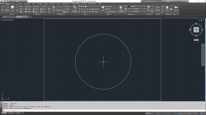
You will need to utilize AutoCAD for the cloning process.
Source: Wikimedia Commons
Open AUTOCAD and create a file. To do this, click on the insert menu and select the raster image. Afterward, select the desired image for this project. The insert image box will then display. Once you insert an image, draw a rectangular frame for the PCB’s border. Ensure that you utilize the object lock point for tracking purposes when creating the structure.
Step three:
First, calculate the number of packages the board contains as you draw the component package. Every package must include one drawing for the board. Then, process it in PORTE99. Afterward, produce the component package and shape.
Step four:
Start the PROTEL99 program and create a PCB file. Then import the CAD file via the PROTEL99 PCB editor menu. A graph representing the component packaging will show up in the editor.
Step five:
Open another PCB component editor in PROTEL99. Pick a component in the PROTEL99 editor and place it in the component editor.
Step six:
Once complete, put every component package in the PROTEL99 editor. After that, you will need to send each one to a CAD file.
Step seven:
Open both the imported and newly created CAD files. Duplicate the newly created CAD file’s component package into the CAD file containing the PCB image.
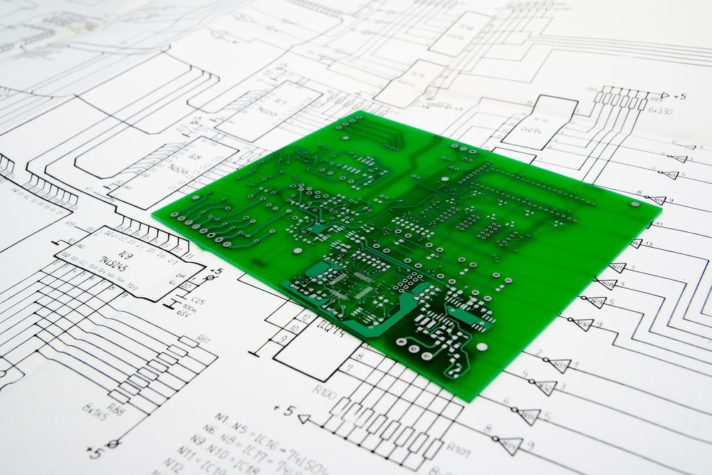
A printed circuit board and schematic
Step eight:
Next, add the pads and vias. Ensure that you measure the inner internal and external diameters. Afterward, open the drawing menu and choose the circle sub-item. You will need to calculate the ring’s inner and outer dimensions. Also, make sure you place each pad based on its size. Additionally, you won’t be able to place both the square and polygon pads. Use the filling method in CAD instead.
Step nine:
Select the aggregate line via the drawing menu to draw the trace. Then, you can add the silkscreen. An irregular screen means you will need the polymer line instead.
Although the entire process seems straightforward, you will need to exercise caution to ensure a proper build. Overall, this project proved beneficial now that we covered all the steps involved with PCB board duplication.
Summary
PCB cloning services, which rely on reverse research technology, offer an excellent and alternative solution for circuit board redesign. Therefore, you will need the original PCB files to achieve this, including the layout. As a result, you won’t have to deal with the hassle of creating a circuit board with new schematics. This reverse engineering service works well with a multilayer and copper layer board. Not only that, but this technique also makes it possible to develop a fully functional circuit board without creating the product from scratch.
Do you have any questions regarding the PCB clone? Feel free to contact us!